KiCad projects often need symbols and footprints that aren’t in the standard library.
Prerequisites
- Basic Circuit Theory
- Baseline understanding of KiCad UI/Workflow
Creating Symbol Libraries
You create symbol libraries in the Symbol Editor. Open it from the Schematic Editor or the KiCad project’s main page.
From the Schematic Editor: navigate to Tools -> Symbol Editor
From the KiCad Project Menu: click into “Symbol Editor” under “Schematic Editor”
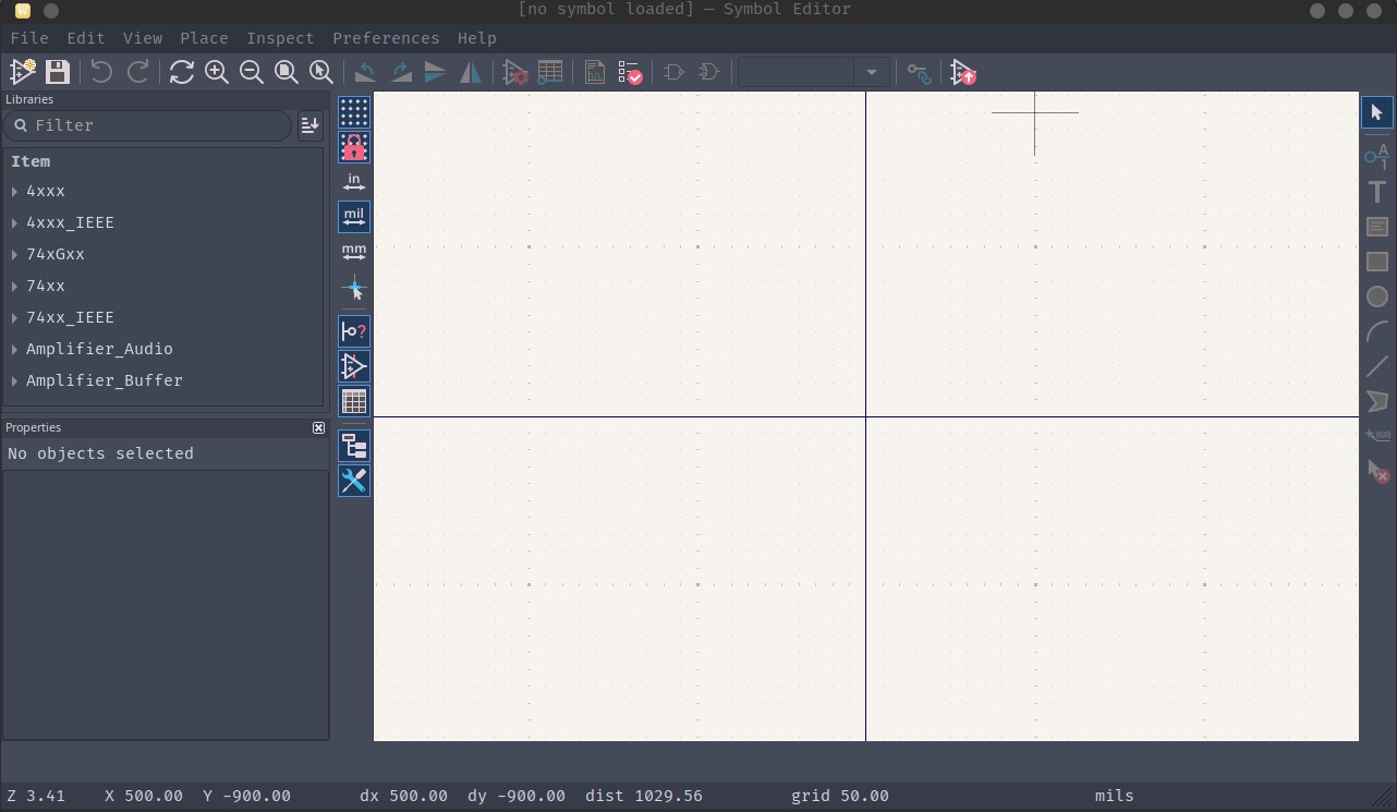
To create a new library, go to File -> New Library
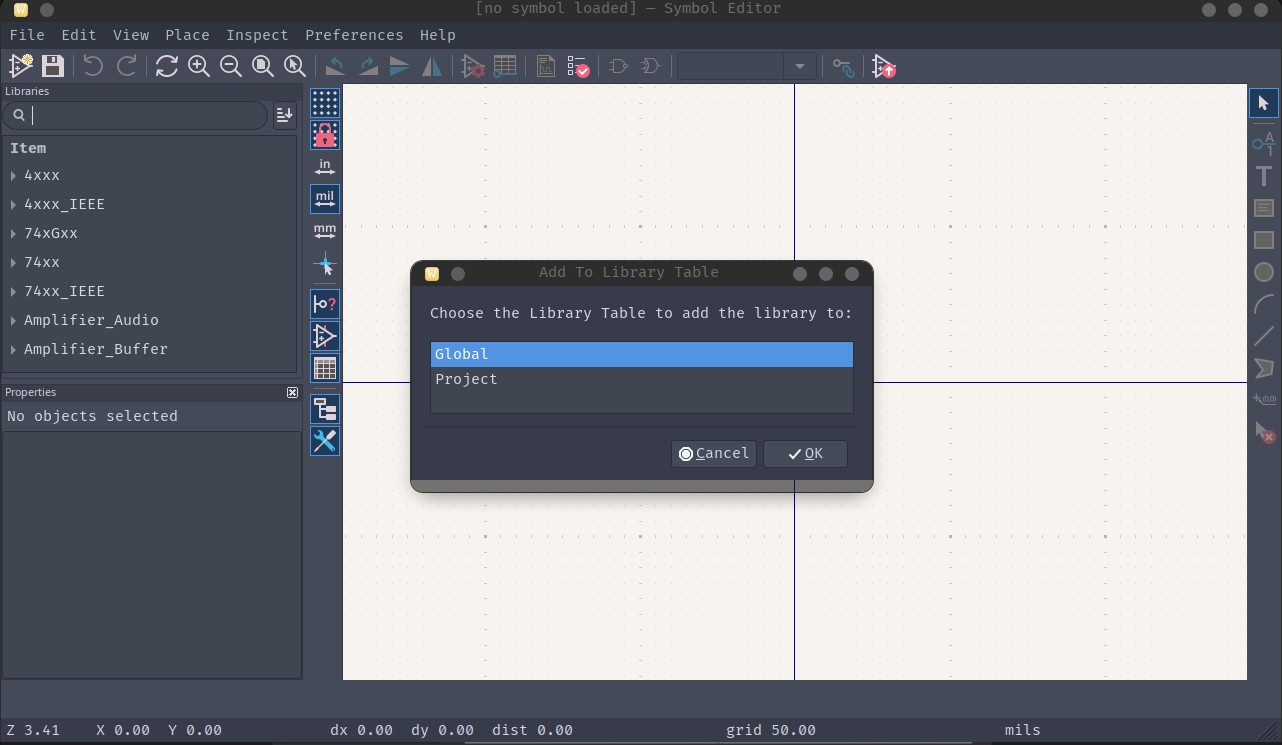
Global libraries are available to any project on the same system. Project libraries are only available in the current project. Use project libraries over global libraries to keep your project portable.
Find a location to place the kicad_sym file, your library. For project libraries, put this file in a local project directory. We usually use a “lib” folder inside the project folder.
Once you’ve created and placed the library, you can create symbols and add them to it.
Creating Custom Symbols
The Symbol Editor
All of this happens in the Symbol Editor. It’s complex and feature rich.
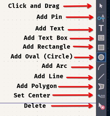
On the right side is a toolbox with all the tools you’ll use for this process.
In the Symbol Editor, create a new symbol with Command+N or Ctrl+N.
Naming the Symbol
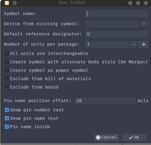
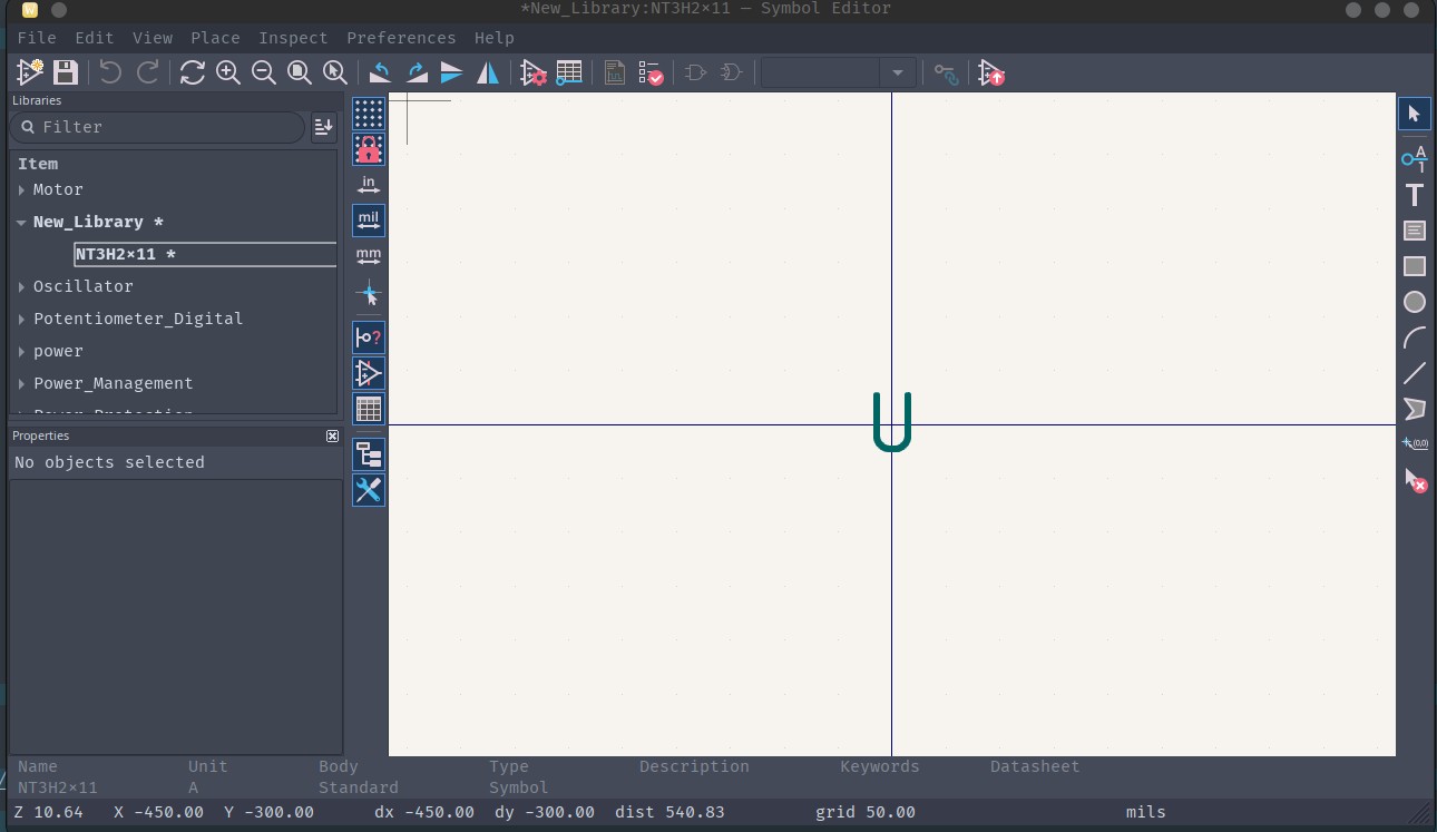
Name the symbol the name of the component you want to add. The reference designator must be added to indicate the type of component. These follow IEEE 315 / ASME Y14.44 conventions:
- AT: Attenuator
- BR: Bridge rectifier
- BT: Battery
- C: Capacitor
- CN: Capacitor network
- D: Diode (including zeners, thyristors and LEDs)
- DL: Delay line
- DS: Display
- F: Fuse
- FB or FEB: Ferrite bead
- FD: Fiducial
- J: Jack connector (female)
- JP: Link (Jumper)
- K: Relay
- L: Inductor
- LS: Loudspeaker or buzzer
- M: Motor
- MK: Microphone
- MP: Mechanical part (including screws and fasteners)
- P: Plug connector (male)
- PS: Power supply
- Q: Transistor (all types)
- R: Resistor
- RN: Resistor network
- RT: Thermistor
- RV: Varistor
- S: Switch (all types, including push-buttons)
- T: Transformer
- TC: Thermocouple
- TUN: Tuner
- TP: Test point
- U: Integrated circuit
- V: Vacuum Tube
- VR: Variable Resistor (potentiometer or rheostat)
- X: Transducer not matching any other category
- Y: Crystal or oscillator
- Z: Zener Diode
Once you’ve done that, it looks like this:
Defining the Symbol Shape
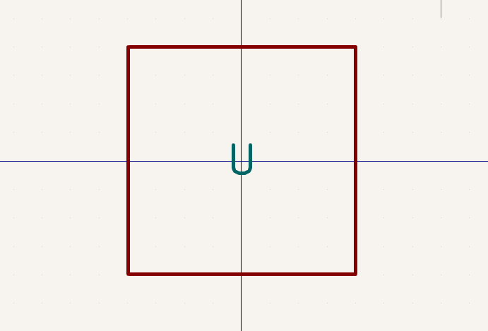
The first step is defining the symbol’s shape or outline. Use the polygon or oval tools to draw a shape to add pins to. Rectangular bodies are the standard, but any shape works.
Adding Pins
The next step is to add the pins. If there are a lot of them, resize the body shape to fit.
There are a number of different pin types in KiCad:
- Power Input: This pin receives power from an external source (e.g. a VDD pin on a micro controller)
- Power Output: This pin supplies power to an external sink (e.g. VIN pin on a DC Jack)
- Input: This pin receives digital signals from an external source (e.g. Reset pin on an MCU)
- Output: This pin sends digital signals to an external sink (e.g. Status pin on an MCU)
- Bidirectional: This pin sends and receives digital signals (e.g. USB D+ and D- pins on an MCU)
- Tri-State: This pin can be input, output or high-Z (floating) (e.g. GPIO in general)
- Passive: This pin does not strongly interact with anything (e.g. A pin on a resistor)
- Free: This pin is floating (e.g. Extraneous pins)
- Unspecified: It is not known what this pin does
- Open Collector: This pin needs a pull up resistor to operate correctly (e.g. SDA and SCL on I2C)
- Open Emitter: This pin needs a pull down resistor to operate correctly
- Unconnected: This pin should not be connected to anything (e.g. Some thermal pads)
Define the type for every pin in your symbol. These definitions help KiCad understand how the design fits together, and they let ERC (Electrical Rules Checking) catch connection errors early.
Check the datasheet for this pin information on the device you’re designing the symbol for. It lists the pin number for every pin. Use that when you place the pins.
Once you have created a Pin, move it and rotate it (using “R”) so that the pin name is inside of the design:
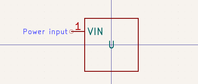
We recommend following these pin placement guidelines:
- All Input Power (VCC, VDD, VIN, etc) should be either on the top of the symbol or the left side
- All Ground (VSS, VEE, GND, etc) should be either on the bottom or the left side of the symbol
- All Inputs should be on the left side of the symbol
- All Outputs should be on the right side of the symbol (this includes power outputs)
- Pins should be organized logically rather than numerically (i.e. put related pins next to each other)
- Pins should be separated by class (i.e. put extra spacing between groups of related pins)
Follow these guidelines and symbols become easier to parse and work with in the schematic.
Once you’ve defined and placed all your pins, modify the symbol properties. Press “E” while nothing is selected in the Symbol Editor.
Defining Symbol Properties
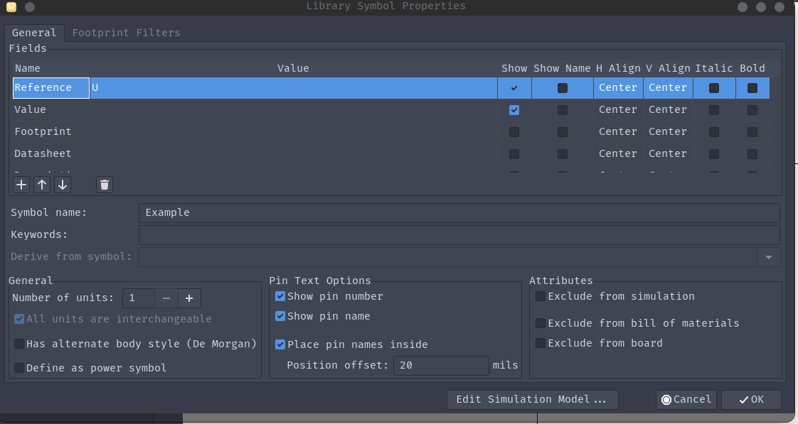
Add the name to the value field, a datasheet link to the datasheet field, a short description to the description field, and the footprint if one already exists.
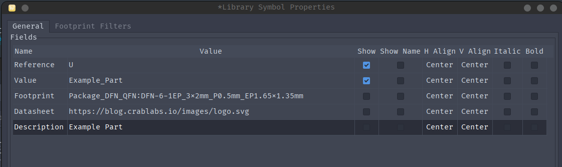
Once you’ve defined the symbol fields and cross-checked the symbol against the datasheet, apply the finishing touches.
Finishing Symbols
Apply coloring to the symbol by clicking the outline polygon and pressing “E”
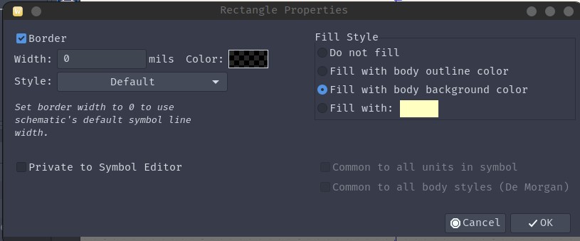
The default coloring for KiCad symbols is “Fill With Body Background Colors,” which works for most cases.
Once you’ve set the coloring, press “Ctrl+S” or “Command+S” to save the symbol to a library.
Custom Symbol Example
We’ll create a symbol for a new component, the NT3H2 NFC Tag by NXP. The datasheet has a pinout diagram for the available packages. We’ll pick the TSSOP-8 package.
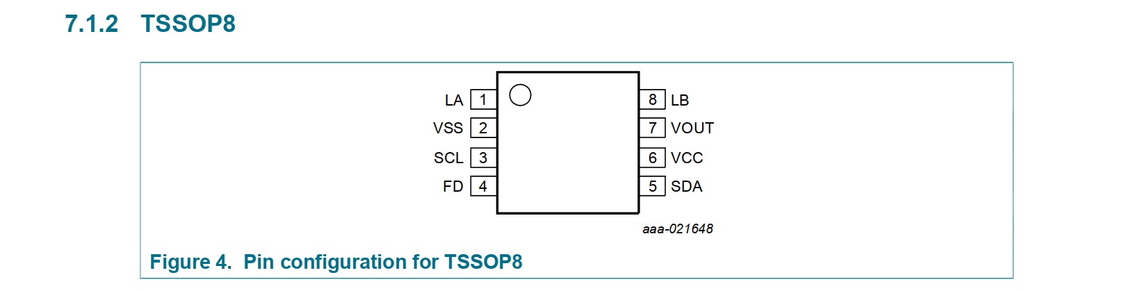
With the pin description in hand, we can start creating the symbol.
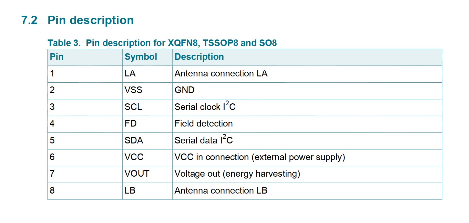
The pinout is the same across all packages (same pin number, same function), so this symbol works for any of the footprints.
We name the symbol “NT3H2x11,” reflecting the full name of the chip. The x represents the different memory variants.
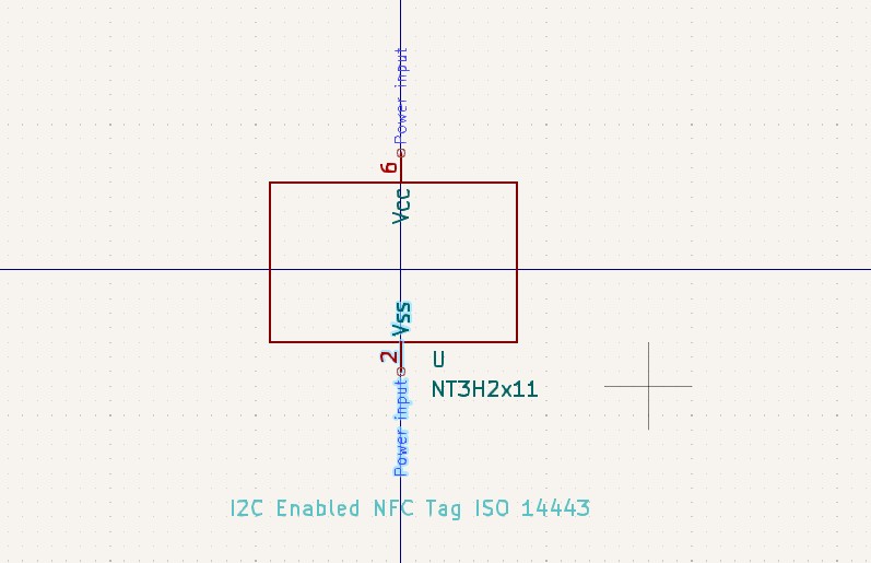
We modify the symbol properties to include information about the component, then add the pins. First VCC (Pin 6, Power Input), then VSS (Pin 2, Power Input). Both receive power from another source, so they’re inputs.
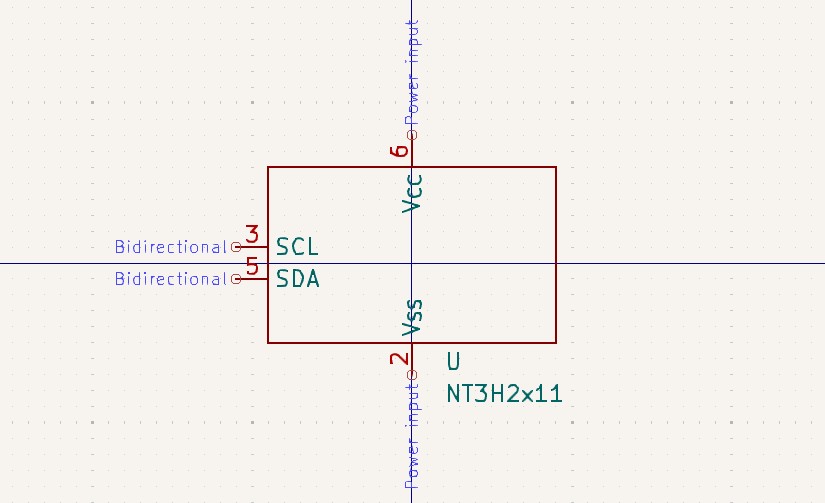
Next, the I2C pins (SDA and SCL). These are bidirectional, though they could also be open collector.
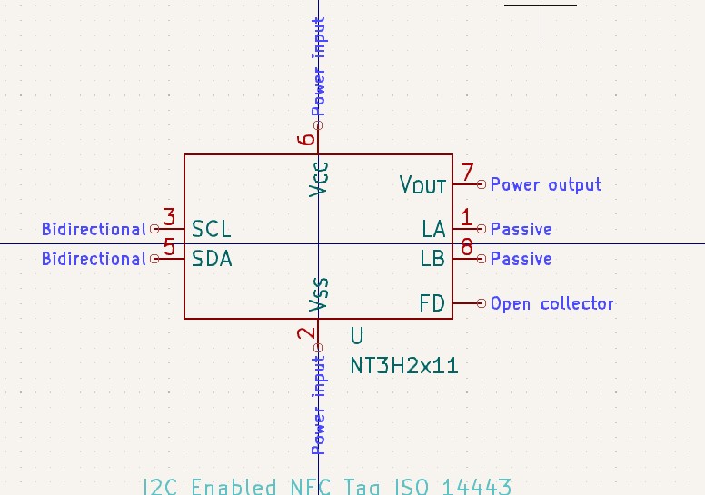
After that, we add the RF circuitry (FD, LA, LB and VOUT). LA and LB are passive since they’re analog signals. FD is open-drain (open collector) and VOUT is power output.
Now we fix the coloration of the rectangle:
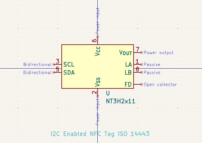
Save the symbol and it’s ready to use in a project.
Creating Footprint Libraries
Creating footprint libraries works the same way as symbol libraries, just in the Footprint Editor instead.
Opening the Footprint Editor
From the PCB Editor: navigate to Tools -> Footprint Editor
From the KiCad Project Menu: click into “Footprint Editor” under “PCB Editor”
Creating a New Footprint Library
In the Footprint Editor:
- Go to File -> New Library
- Choose between Global and Project libraries (Project is recommended)
- Save the .pretty folder in your project directory
Creating Custom Footprints
Basic Footprint Creation Steps
- Create a new footprint: Use Ctrl+N or Command+N
- Name the footprint: Follow IPC naming conventions when possible
- Add pads: Place and configure pads according to the datasheet
- Add silkscreen: Draw component outline and reference designator
- Add courtyard: Define the component’s keep-out area
- Add 3D model: Optional but helpful for visualization
Pad Properties
Important pad properties to configure:
- Pad type: Through-hole, SMD or NPTH (non-plated through-hole)
- Shape: Circular, rectangular, oval or custom
- Size: Follow datasheet recommendations
- Drill size: For through-hole components
- Layers: Which copper layers the pad appears on
- Clearance: Spacing from other copper features
- Thermal relief: For connections to planes
Design Rules
Follow these guidelines for reliable footprints:
- Pad size: Generally 0.2-0.3mm larger than lead dimensions
- Courtyard: Minimum 0.25mm clearance around component body
- Silkscreen: Keep 0.2mm away from pads (per KLC requirements)
- Reference designator: Should be clearly visible after assembly
- Pin 1 marking: Always indicate pin 1 orientation
Footprint Wizard
KiCad includes footprint wizards for common package types:
- In Footprint Editor, go to File -> Footprint Wizard
- Select the appropriate wizard (QFP, SOIC, etc.)
- Enter package dimensions from datasheet
- Review and adjust the generated footprint
- Save to your library
Verifying Footprints
Always verify your footprints before use:
- Print at 1:1 scale: Place actual component on printout
- Check against datasheet: Verify all dimensions
- 3D viewer: Use View -> 3D Viewer to check appearance
- DRC check: Run design rules check in PCB editor
- Test board: Consider ordering a test PCB for critical designs
Managing Libraries
Library Tables
KiCad uses library tables to manage symbol and footprint libraries:
- Global libraries: Available to all projects
- Project libraries: Specific to current project
Access library tables through:
- Preferences -> Manage Symbol Libraries
- Preferences -> Manage Footprint Libraries
Library Organization Tips
- Separate by function: Group related components
- Version control: Track library changes
- Documentation: Include datasheets and notes
- Naming convention: Use consistent, descriptive names
- Backup regularly: Libraries represent significant work
Sharing Libraries
To share libraries with team members:
- Use relative paths in library tables
- Include libraries in version control
- Document any special requirements
- Consider using library management tools
Advanced Topics
Multi-Unit Symbols
For complex components with multiple functional units:
- Create symbol with multiple units
- Define power pins as common to all units
- Use unit suffixes (U1A, U1B, etc.)
Alternate Pin Functions
For microcontrollers with multiple pin functions:
- Use stacked pin names (e.g., “PA0/TXD/INT0”)
- Consider creating alternate symbol versions
- Document pin functions in symbol fields
Custom Pad Shapes
For special requirements:
- Use pad primitives to build complex shapes
- Consider thermal and mechanical requirements
- Verify with manufacturer capabilities
Library Automation
For large-scale library creation:
- Use KiCad’s Python scripting API
- Import from manufacturer data
- Consider tools like KiPart or csv2kicad
- Validate automated results carefully
Common Pitfalls
Incorrect pin numbering causes wrong connections. Verify against the datasheet, not the part’s marking or a prior revision. Wrong pad dimensions cause assembly issues that only show up at the assembly house. A missing courtyard triggers DRC errors. Incorrect layer assignments (pad vs. silkscreen) and a missing 3D model both make the part harder to place and verify. Poor organization is the slow failure: a library that’s hard to navigate gets duplicated instead of reused, and the duplicates drift apart.
Follow IPC standards for footprints and IEEE 315 for reference designators, keep the library under version control, and verify every new part against a prototype before it goes into a production run.
More on the tools we standardize on: our capabilities page.